graphene:electronic_structure
This is an old revision of the document!
Band structure plot
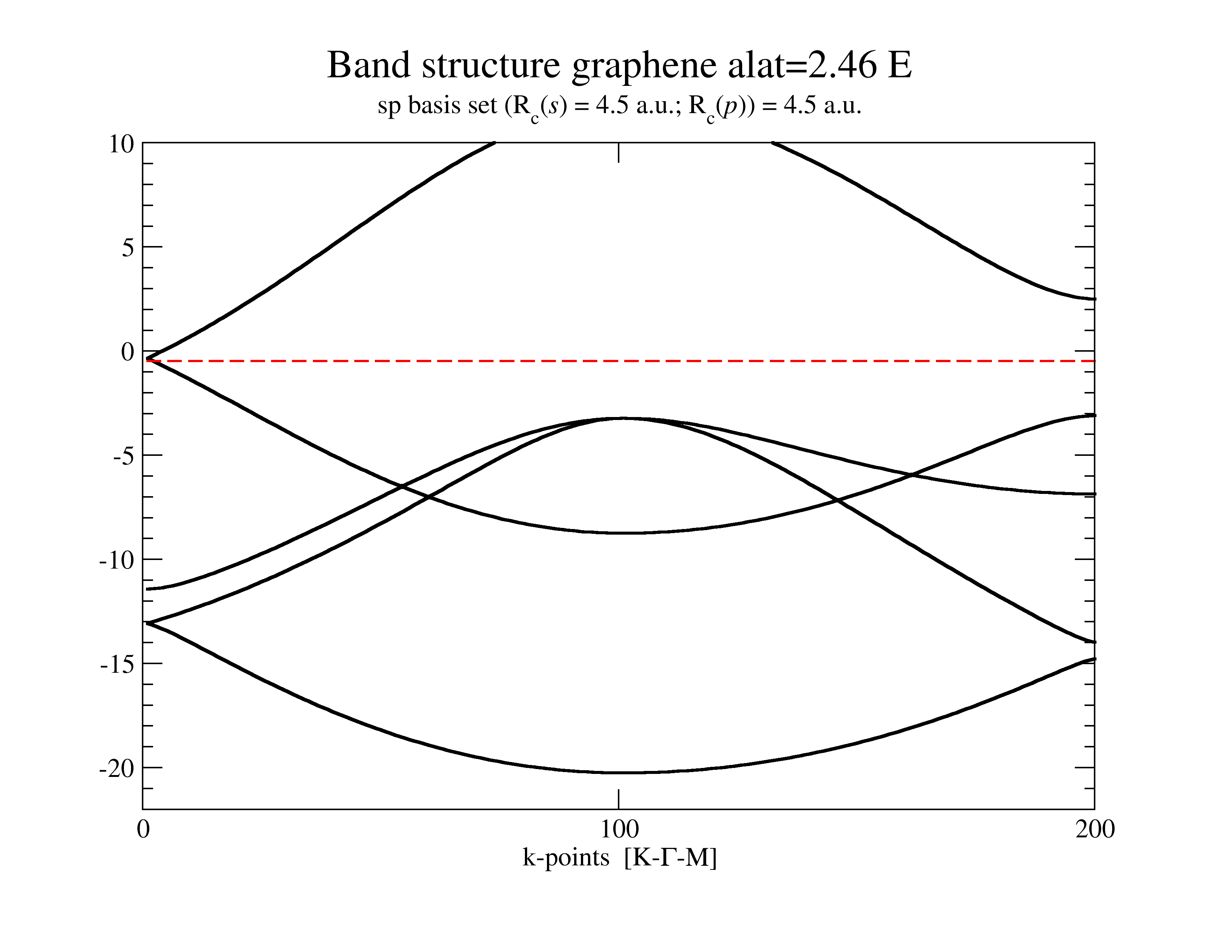
In previous section we optimized the lattice parameter of graphene. In this section we show how to generate the band structure at given high-symmetry directions. We follow the same procedure as in the previous case of the Silicon bulk:
Procedure
- obtain the SCF charges
- generate a set of special high symmetry k-points
- get eigenvalue spectra with fixed SCF charges & the set of high symmetry k-points
- plot eigenvalue vs. k-points
To plot the band structure we generated a set of the special k-points heading from K(1/√3,1/3) point to Γ(0,0) ending at M(0,2/3) stored in file C1.kgm.kpts.
Real space electron denisty
Another way to analyze the electronic structure of material is a plot of electron density in real space. This kind of analysis can be compared, with certain caution, with STM images. To obtain this image we have to proceed following steps:
- obtain the SCF charges
- plot wavefunction in real-space
graphene/electronic_structure.1267266964.txt.gz · Last modified: 2011/02/18 13:14 (external edit)


